Timers
the timer is controlled by setting bits in the timer configuration registers.
then you have to define the ISR (interrupt service routines)
to get the timed behaviour.
Starting the timer
to start timer 0 you have to select the clock to use:
set the CS0
Clock Select
Select Between Internal Clock with prescaler
and external Clock on T0 (rising or falling edge)
CS02
TCCR0B[2] |
CS01
TCCR0B[1] |
CS00
TCCR0B[0] |
|
| 0 |
0 |
0 |
off |
| 0 |
0 |
1 |
1x ⌚ |
| 0 |
1 |
0 |
8x ⌚ |
| 0 |
1 |
1 |
64x ⌚ |
| 1 |
0 |
0 |
256x ⌚ |
| 1 |
0 |
1 |
1024x ⌚ |
| 1 |
1 |
0 |
T0 ↳. |
| 1 |
1 |
1 |
T0 ↱. |
bits in TCCR0B
Timer/Counter 0 Control Register B
| 7 |
6 |
5 |
4 |
3 |
2 |
1 |
0 |
| FOC0A |
FOC0B |
..... |
..... |
WGM02 |
.CS02 |
.CS01 |
.CS00 |
| FOC0x |
WGM0[2:0] |
CS0[2:0] |
| Force Output Compare 0 A/B |
Waveform Generation Mode |
Clock Select |
// start internal clock without prescaler
TCCR0B
Timer/Counter 0 Control Register B
| 7 |
6 |
5 |
4 |
3 |
2 |
1 |
0 |
| FOC0A |
FOC0B |
..... |
..... |
WGM02 |
.CS02 |
.CS01 |
.CS00 |
| FOC0x |
WGM0[2:0] |
CS0[2:0] |
| Force Output Compare 0 A/B |
Waveform Generation Mode |
Clock Select |
|= (1 << CS0
Clock Select
Select Between Internal Clock with prescaler
and external Clock on T0 (rising or falling edge)
CS02
TCCR0B[2] |
CS01
TCCR0B[1] |
CS00
TCCR0B[0] |
|
| 0 |
0 |
0 |
off |
| 0 |
0 |
1 |
1x ⌚ |
| 0 |
1 |
0 |
8x ⌚ |
| 0 |
1 |
1 |
64x ⌚ |
| 1 |
0 |
0 |
256x ⌚ |
| 1 |
0 |
1 |
1024x ⌚ |
| 1 |
1 |
0 |
T0 ↳. |
| 1 |
1 |
1 |
T0 ↱. |
0);
// or TCCR0B
Timer/Counter 0 Control Register B
| 7 |
6 |
5 |
4 |
3 |
2 |
1 |
0 |
| FOC0A |
FOC0B |
..... |
..... |
WGM02 |
.CS02 |
.CS01 |
.CS00 |
| FOC0x |
WGM0[2:0] |
CS0[2:0] |
| Force Output Compare 0 A/B |
Waveform Generation Mode |
Clock Select |
|= 0x01;
// start internal clock with prescaler 1024
TCCR0B
Timer/Counter 0 Control Register B
| 7 |
6 |
5 |
4 |
3 |
2 |
1 |
0 |
| FOC0A |
FOC0B |
..... |
..... |
WGM02 |
.CS02 |
.CS01 |
.CS00 |
| FOC0x |
WGM0[2:0] |
CS0[2:0] |
| Force Output Compare 0 A/B |
Waveform Generation Mode |
Clock Select |
|= (1 << CS0
Clock Select
Select Between Internal Clock with prescaler
and external Clock on T0 (rising or falling edge)
CS02
TCCR0B[2] |
CS01
TCCR0B[1] |
CS00
TCCR0B[0] |
|
| 0 |
0 |
0 |
off |
| 0 |
0 |
1 |
1x ⌚ |
| 0 |
1 |
0 |
8x ⌚ |
| 0 |
1 |
1 |
64x ⌚ |
| 1 |
0 |
0 |
256x ⌚ |
| 1 |
0 |
1 |
1024x ⌚ |
| 1 |
1 |
0 |
T0 ↳. |
| 1 |
1 |
1 |
T0 ↱. |
2) | (1 << CS0
Clock Select
Select Between Internal Clock with prescaler
and external Clock on T0 (rising or falling edge)
CS02
TCCR0B[2] |
CS01
TCCR0B[1] |
CS00
TCCR0B[0] |
|
| 0 |
0 |
0 |
off |
| 0 |
0 |
1 |
1x ⌚ |
| 0 |
1 |
0 |
8x ⌚ |
| 0 |
1 |
1 |
64x ⌚ |
| 1 |
0 |
0 |
256x ⌚ |
| 1 |
0 |
1 |
1024x ⌚ |
| 1 |
1 |
0 |
T0 ↳. |
| 1 |
1 |
1 |
T0 ↱. |
0);
// or TCCR0B
Timer/Counter 0 Control Register B
| 7 |
6 |
5 |
4 |
3 |
2 |
1 |
0 |
| FOC0A |
FOC0B |
..... |
..... |
WGM02 |
.CS02 |
.CS01 |
.CS00 |
| FOC0x |
WGM0[2:0] |
CS0[2:0] |
| Force Output Compare 0 A/B |
Waveform Generation Mode |
Clock Select |
|= 0x05
to stop the timer you have to clear the clock select bits
// stop clock
TCCR0B
Timer/Counter 0 Control Register B
| 7 |
6 |
5 |
4 |
3 |
2 |
1 |
0 |
| FOC0A |
FOC0B |
..... |
..... |
WGM02 |
.CS02 |
.CS01 |
.CS00 |
| FOC0x |
WGM0[2:0] |
CS0[2:0] |
| Force Output Compare 0 A/B |
Waveform Generation Mode |
Clock Select |
&= ~( (1 << CS0
Clock Select
Select Between Internal Clock with prescaler
and external Clock on T0 (rising or falling edge)
CS02
TCCR0B[2] |
CS01
TCCR0B[1] |
CS00
TCCR0B[0] |
|
| 0 |
0 |
0 |
off |
| 0 |
0 |
1 |
1x ⌚ |
| 0 |
1 |
0 |
8x ⌚ |
| 0 |
1 |
1 |
64x ⌚ |
| 1 |
0 |
0 |
256x ⌚ |
| 1 |
0 |
1 |
1024x ⌚ |
| 1 |
1 |
0 |
T0 ↳. |
| 1 |
1 |
1 |
T0 ↱. |
2) | (1 << CS0
Clock Select
Select Between Internal Clock with prescaler
and external Clock on T0 (rising or falling edge)
CS02
TCCR0B[2] |
CS01
TCCR0B[1] |
CS00
TCCR0B[0] |
|
| 0 |
0 |
0 |
off |
| 0 |
0 |
1 |
1x ⌚ |
| 0 |
1 |
0 |
8x ⌚ |
| 0 |
1 |
1 |
64x ⌚ |
| 1 |
0 |
0 |
256x ⌚ |
| 1 |
0 |
1 |
1024x ⌚ |
| 1 |
1 |
0 |
T0 ↳. |
| 1 |
1 |
1 |
T0 ↱. |
1) | (1 << CS0
Clock Select
Select Between Internal Clock with prescaler
and external Clock on T0 (rising or falling edge)
CS02
TCCR0B[2] |
CS01
TCCR0B[1] |
CS00
TCCR0B[0] |
|
| 0 |
0 |
0 |
off |
| 0 |
0 |
1 |
1x ⌚ |
| 0 |
1 |
0 |
8x ⌚ |
| 0 |
1 |
1 |
64x ⌚ |
| 1 |
0 |
0 |
256x ⌚ |
| 1 |
0 |
1 |
1024x ⌚ |
| 1 |
1 |
0 |
T0 ↳. |
| 1 |
1 |
1 |
T0 ↱. |
0) );
// or TCCR0B
Timer/Counter 0 Control Register B
| 7 |
6 |
5 |
4 |
3 |
2 |
1 |
0 |
| FOC0A |
FOC0B |
..... |
..... |
WGM02 |
.CS02 |
.CS01 |
.CS00 |
| FOC0x |
WGM0[2:0] |
CS0[2:0] |
| Force Output Compare 0 A/B |
Waveform Generation Mode |
Clock Select |
&= ~0x07;
Generating a PWM signal
to generate a PWM signal we set OCR0A
Output Compare Register A
to the desired duty cycle
so the output is HIGH until we get a compare match and then Low until we hit a timer overflow
#define F_CPU 16000000
#include <avr/io.h>
#include <util/delay.h>
#include <avr/interrupt.h>
int main(){
TCCR0A
Timer/Counter 0 Control Register A
| 7 |
6 |
5 |
4 |
3 |
2 |
1 |
0 |
| COM0A1 |
COM0A0 |
COM0B1 |
COM0B0 |
...... |
...... |
WGM01. |
WGM00. |
| COM0xn |
WGM0[2:0] |
| Compare Match Output A/B Mode |
Waveform Generation Mode |
= (1 << COM0A1) | (1<<WGM01) | (1<<WGM00);
TCCR0B
Timer/Counter 0 Control Register B
| 7 |
6 |
5 |
4 |
3 |
2 |
1 |
0 |
| FOC0A |
FOC0B |
..... |
..... |
WGM02 |
.CS02 |
.CS01 |
.CS00 |
| FOC0x |
WGM0[2:0] |
CS0[2:0] |
| Force Output Compare 0 A/B |
Waveform Generation Mode |
Clock Select |
= (1 << CS0
Clock Select
Select Between Internal Clock with prescaler
and external Clock on T0 (rising or falling edge)
CS02
TCCR0B[2] |
CS01
TCCR0B[1] |
CS00
TCCR0B[0] |
|
| 0 |
0 |
0 |
off |
| 0 |
0 |
1 |
1x ⌚ |
| 0 |
1 |
0 |
8x ⌚ |
| 0 |
1 |
1 |
64x ⌚ |
| 1 |
0 |
0 |
256x ⌚ |
| 1 |
0 |
1 |
1024x ⌚ |
| 1 |
1 |
0 |
T0 ↳. |
| 1 |
1 |
1 |
T0 ↱. |
2) | (1 << CS0
Clock Select
Select Between Internal Clock with prescaler
and external Clock on T0 (rising or falling edge)
CS02
TCCR0B[2] |
CS01
TCCR0B[1] |
CS00
TCCR0B[0] |
|
| 0 |
0 |
0 |
off |
| 0 |
0 |
1 |
1x ⌚ |
| 0 |
1 |
0 |
8x ⌚ |
| 0 |
1 |
1 |
64x ⌚ |
| 1 |
0 |
0 |
256x ⌚ |
| 1 |
0 |
1 |
1024x ⌚ |
| 1 |
1 |
0 |
T0 ↳. |
| 1 |
1 |
1 |
T0 ↱. |
0);
// example atmega328
// set pwm pin to output
// consult the specific Datasheet for which pin to use
DDRD = (1<<6);
while (1){
OCR0A
Output Compare Register A
+= 1;
_delay_ms(1);
}
}
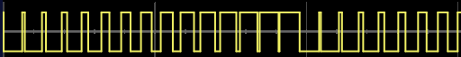
This is the output signal on OC0A:
Appendix
| Register |
Description |
| Config |
|
TCCR0A
Timer/Counter 0 Control Register A
| 7 |
6 |
5 |
4 |
3 |
2 |
1 |
0 |
| COM0A1 |
COM0A0 |
COM0B1 |
COM0B0 |
...... |
...... |
WGM01. |
WGM00. |
| COM0xn |
WGM0[2:0] |
| Compare Match Output A/B Mode |
Waveform Generation Mode |
|
Timer/Counter 0 control register A |
TCCR0B
Timer/Counter 0 Control Register B
| 7 |
6 |
5 |
4 |
3 |
2 |
1 |
0 |
| FOC0A |
FOC0B |
..... |
..... |
WGM02 |
.CS02 |
.CS01 |
.CS00 |
| FOC0x |
WGM0[2:0] |
CS0[2:0] |
| Force Output Compare 0 A/B |
Waveform Generation Mode |
Clock Select |
|
Timer/Counter 0 control register B |
| |
|
| # Compare |
|
| OCR0A
Output Compare Register A
|
Timer/Counter 0 output compare register A |
| OCR0B
Output Compare Register B
|
Timer/Counter 0 output compare register B |
| |
|
| Value |
|
| TCNT0 |
holds the current value of the timer |
TC0
Timer/Counter 0
TCCR0A
Timer/Counter 0 Control Register A
| 7 |
6 |
5 |
4 |
3 |
2 |
1 |
0 |
| COM0A1 |
COM0A0 |
COM0B1 |
COM0B0 |
...... |
...... |
WGM01. |
WGM00. |
| COM0xn |
WGM0[2:0] |
| Compare Match Output A/B Mode |
Waveform Generation Mode |
TCCR0B
Timer/Counter 0 Control Register B
| 7 |
6 |
5 |
4 |
3 |
2 |
1 |
0 |
| FOC0A |
FOC0B |
..... |
..... |
WGM02 |
.CS0
Clock Select
Select Between Internal Clock with prescaler
and external Clock on T0
rising or falling edge
CS02
TCCR0B[2] |
CS01
TCCR0B[1] |
CS00
TCCR0B[0] |
|
| 0 |
0 |
0 |
off |
| 0 |
0 |
1 |
1x ⌚ |
| 0 |
1 |
0 |
8x ⌚ |
| 0 |
1 |
1 |
64x ⌚ |
| 1 |
0 |
0 |
256x ⌚ |
| 1 |
0 |
1 |
1024x ⌚ |
| 1 |
1 |
0 |
T0 ↳. |
| 1 |
1 |
1 |
T0 ↱. |
2 |
.CS0
Clock Select
Select Between Internal Clock with prescaler
and external Clock on T0
rising or falling edge
CS02
TCCR0B[2] |
CS01
TCCR0B[1] |
CS00
TCCR0B[0] |
|
| 0 |
0 |
0 |
off |
| 0 |
0 |
1 |
1x ⌚ |
| 0 |
1 |
0 |
8x ⌚ |
| 0 |
1 |
1 |
64x ⌚ |
| 1 |
0 |
0 |
256x ⌚ |
| 1 |
0 |
1 |
1024x ⌚ |
| 1 |
1 |
0 |
T0 ↳. |
| 1 |
1 |
1 |
T0 ↱. |
1 |
.CS0
Clock Select
Select Between Internal Clock with prescaler
and external Clock on T0
rising or falling edge
CS02
TCCR0B[2] |
CS01
TCCR0B[1] |
CS00
TCCR0B[0] |
|
| 0 |
0 |
0 |
off |
| 0 |
0 |
1 |
1x ⌚ |
| 0 |
1 |
0 |
8x ⌚ |
| 0 |
1 |
1 |
64x ⌚ |
| 1 |
0 |
0 |
256x ⌚ |
| 1 |
0 |
1 |
1024x ⌚ |
| 1 |
1 |
0 |
T0 ↳. |
| 1 |
1 |
1 |
T0 ↱. |
0 |
| FOC0x |
WGM0[2:0] |
CS0
Clock Select
Select Between Internal Clock with prescaler
and external Clock on T0
rising or falling edge
CS02
TCCR0B[2] |
CS01
TCCR0B[1] |
CS00
TCCR0B[0] |
|
| 0 |
0 |
0 |
off |
| 0 |
0 |
1 |
1x ⌚ |
| 0 |
1 |
0 |
8x ⌚ |
| 0 |
1 |
1 |
64x ⌚ |
| 1 |
0 |
0 |
256x ⌚ |
| 1 |
0 |
1 |
1024x ⌚ |
| 1 |
1 |
0 |
T0 ↳. |
| 1 |
1 |
1 |
T0 ↱. |
[2:0] |
| Force Output Compare 0 A/B |
Waveform Generation Mode |
Clock Select |
CS0
Clock Select
Select Between Internal Clock with prescaler
and external Clock on T0 (rising or falling edge)
CS02
TCCR0B
Timer/Counter 0 Control Register B
| 7 |
6 |
5 |
4 |
3 |
2 |
1 |
0 |
| FOC0A |
FOC0B |
..... |
..... |
WGM02 |
.CS02 |
.CS01 |
.CS00 |
| FOC0x |
WGM0[2:0] |
CS0[2:0] |
| Force Output Compare 0 A/B |
Waveform Generation Mode |
Clock Select |
[2] |
CS01
TCCR0B
Timer/Counter 0 Control Register B
| 7 |
6 |
5 |
4 |
3 |
2 |
1 |
0 |
| FOC0A |
FOC0B |
..... |
..... |
WGM02 |
.CS02 |
.CS01 |
.CS00 |
| FOC0x |
WGM0[2:0] |
CS0[2:0] |
| Force Output Compare 0 A/B |
Waveform Generation Mode |
Clock Select |
[1] |
CS00
TCCR0B
Timer/Counter 0 Control Register B
| 7 |
6 |
5 |
4 |
3 |
2 |
1 |
0 |
| FOC0A |
FOC0B |
..... |
..... |
WGM02 |
.CS02 |
.CS01 |
.CS00 |
| FOC0x |
WGM0[2:0] |
CS0[2:0] |
| Force Output Compare 0 A/B |
Waveform Generation Mode |
Clock Select |
[0] |
|
| 0 |
0 |
0 |
off |
| 0 |
0 |
1 |
1x ⌚ |
| 0 |
1 |
0 |
8x ⌚ |
| 0 |
1 |
1 |
64x ⌚ |
| 1 |
0 |
0 |
256x ⌚ |
| 1 |
0 |
1 |
1024x ⌚ |
| 1 |
1 |
0 |
T0 ↳. |
| 1 |
1 |
1 |
T0 ↱. |
OCR0A
Output Compare Register A
OCR0B
Output Compare Register B
TIMSK0
Timer/Counter Interrupt Mask Register
TIFR0
| 7 |
6 |
5 |
4 |
3 |
2 |
1 |
0 |
| ..... |
..... |
..... |
..... |
OCF0B
Output Compare Flag 0 B
|
OCF0A
Output Compare Flag 0 A
|
.TOV0
Timer/Counter0 Overflow Flag |
..... |
OCF0B
Output Compare Flag 0 B
OCF0A
Output Compare Flag 0 A
TOV0
Timer/Counter0 Overflow Flag
generated from markdown
source